Infrastructure
Our state-of-the-art facilities are designed to meet the highest standards of quality and efficiency.
Our CIPSA-TEC journey began in December 2005, growing into a leading name in PCB manufacturing. We strengthened our foundation by acquiring the business of RIC, a pioneer in the Indian PCB industry, originally established in 1987 in collaboration with UNICAP, Taiwan.
With a state-of-the-art manufacturing setup, we operate one of the most advanced facilities in the country. Our Tumkur plant, originally a Sanmina setup from Germany, with a 12,000 Sqm built-up area.
As the One-of-the-largest PCB manufacturer in India, we achieved threefold growth from 2005 to 2009, further solidifying our position in the industry.
Inside Our Manufacturing Excellence
Discover how we deliver high-quality PCBs with advanced technology, precision, and efficiency. Our state-of-the-art facility is equipped with the latest European machinery and a highly skilled workforce to ensure superior results.
Process Flow Block Diagram
Our shearing capabilities include advanced equipment:
- Semi-automatic sheet cutters: Ensuring precise cutting of PCB sheets.
- Auto-edge matte machines: Maintaining edge quality and consistency.
Utilizing state-of-the-art CNC drilling machines:
- POSALUX, GIGA, and PLURITEC technologies: Equipped with X-ray capabilities for precise and accurate drilling of holes.
- Ensures optimal alignment and dimensional accuracy in PCB production.
Enhanced de-burring and de-smear capabilities:
- International supplier technologies: Utilized for effective removal of burrs and residues.
- Vertical de-smear lines: Ensuring clean surfaces essential for subsequent PCB processing steps.
Efficient processing of plated through holes:
- Vertical PTH lines: Ensuring reliable electrical connections across PCB layers.
- Enhances the durability and performance of PCBs in various applications.
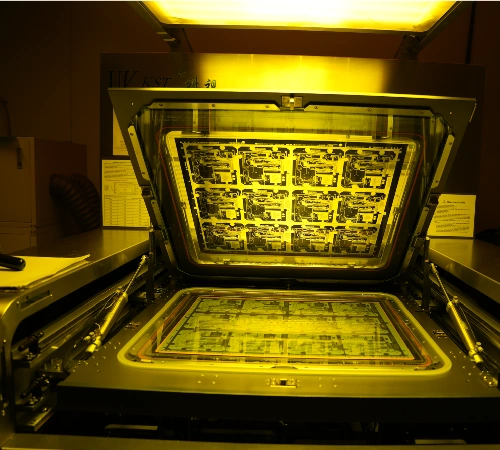
Advanced technologies for precise image transfer:
- UV-SKT and OLEC systems: Ensuring accurate transfer of PCB designs onto substrate materials.
- Supports intricate and detailed PCB layouts required for complex electronic devices.
Specialized capabilities in pattern plating:
- Metezka vertical pattern plating line: Consistently delivers uniform and precise patterning on PCB surfaces.
- Fischer scope: Utilized for precise measurement and quality control during the plating process.
Efficient strip, etch, and strip processes:
- Schmid technologies: Ensuring efficient and controlled processing of PCB layers.
- Enhances the reliability and performance of PCBs through optimized manufacturing processes.
Effective preparation of solder mask surfaces:
- IS Pumice and semi-automatic Thieme printing machines: Used for thorough pre-cleaning of solder mask surfaces.
- ORC exposure: Ensuring precise application and alignment of solder mask materials.
Versatile surface finishing capabilities:
- Utilizing PENTA, Quick Silver, and Sunshine technologies: Offering a range of surface finish options to meet diverse application requirements.
- Enhances PCB durability, solderability, and overall performance in varied environmental conditions.
Precision V-scoring capabilities:
- TELMEC and HRF technologies: Ensuring accurate and clean V-scoring cuts on PCB panels.
- Facilitates efficient PCB separation and assembly processes.
Advanced CNC routing capabilities:
- POSALUX and SCHMOL: Enabling intricate and precise shaping of PCBs according to design specifications.
- Supports the production of complex PCB geometries required for modern electronic devices.
Comprehensive electrical testing capabilities:
- ATG- MAKE EXALINE, MANIA UNIVARSAL BBT: Providing thorough and reliable electrical testing of PCBs.
- Ensures high-quality standards and adherence to specifications before product delivery.
Secure and professional final packing processes:
- KALLFASS automatic vacuum packing machines: Ensuring safe and protective packaging of finished PCB products.
- Enhances product integrity during storage, shipping, and handling.
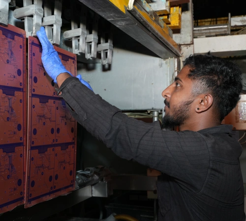
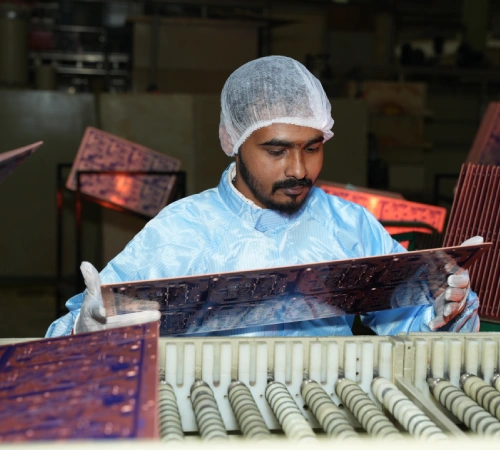
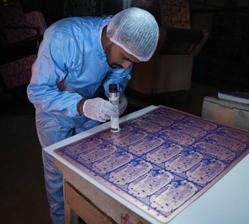
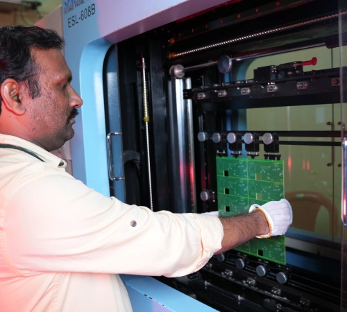
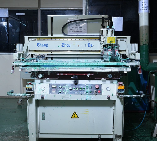
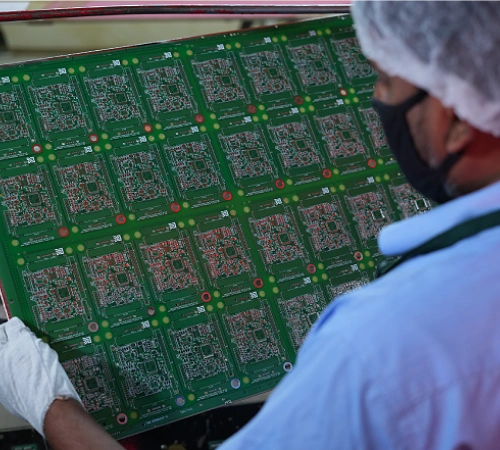
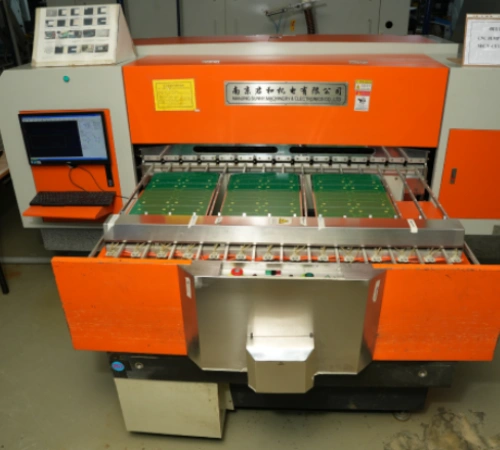
Photo Gallery